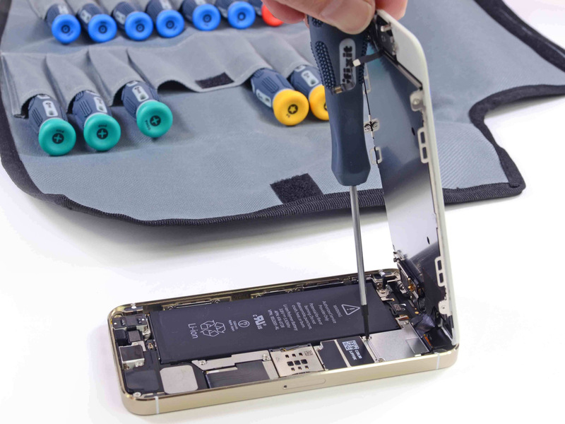
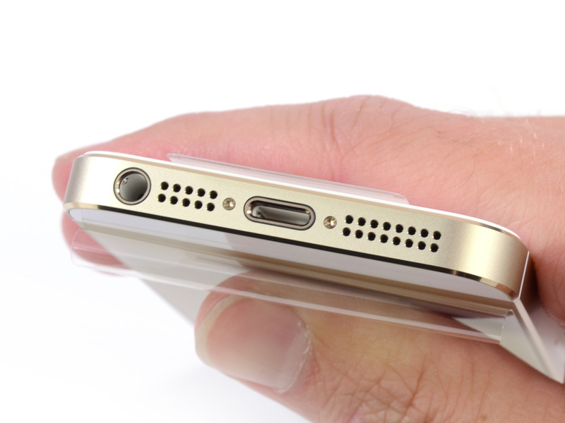
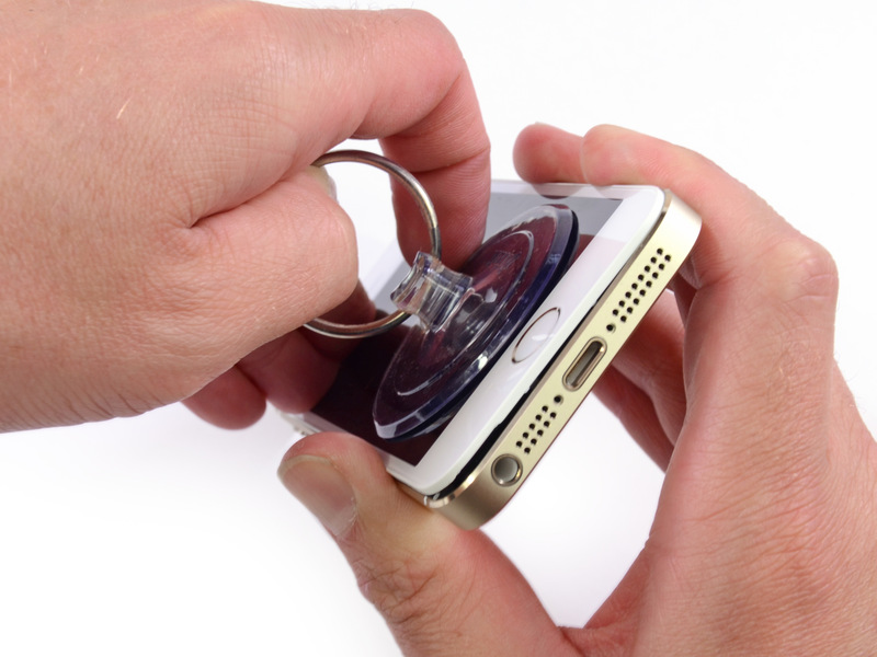
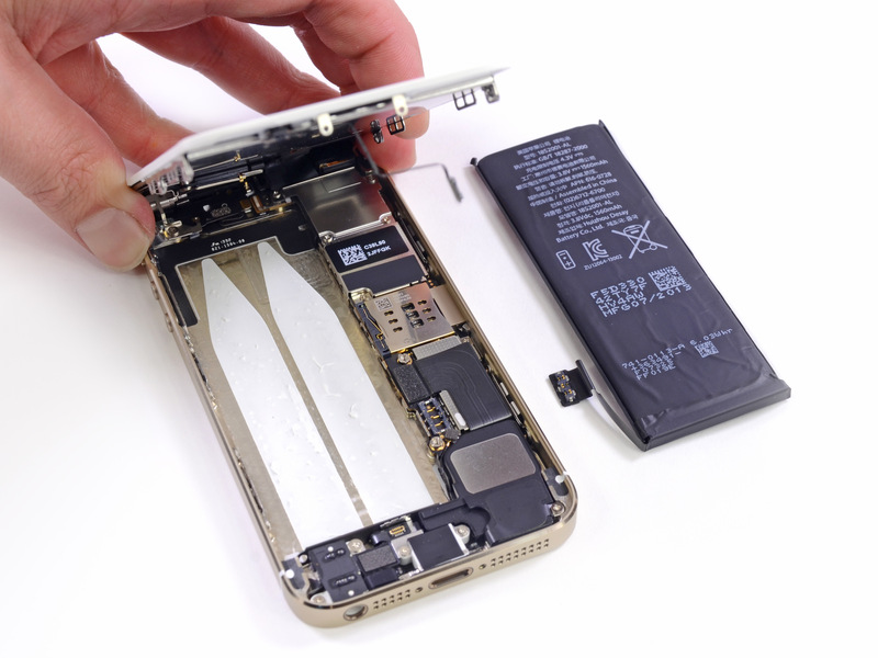
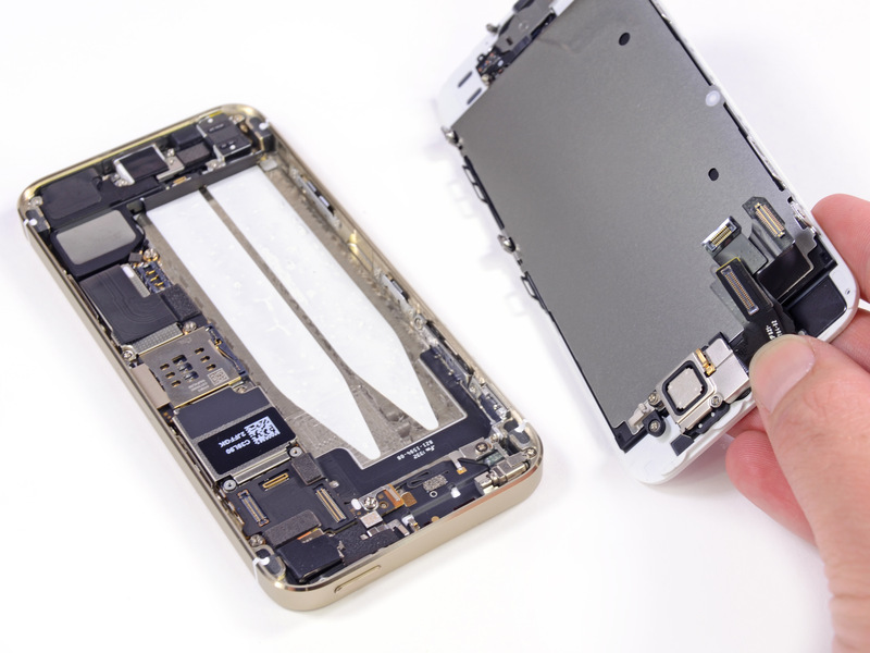
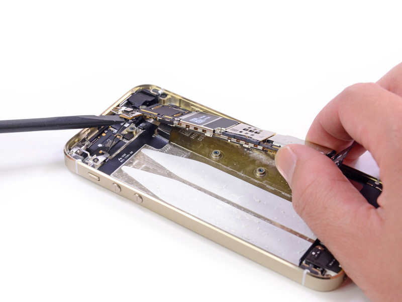
Last night I saw the first teardown of the terminal iPhone 5S, this practically representing a complete disassembly and a presentation of the internal components "hidden" in it. If the first teardown wasn't so informative, well those from iFixIT they did it to get one iPhone 5S golden and shows us in detail all the components hidden inside iPhone 5S. To begin with, the differences between the internal structure of iPhone 5 and that of the iPhone 5S are minor, the arrangement of screws for fixing the components and an additional cable for touch ID being the main news.
Below are all the important changes:
- the battery of the terminal is much more firmly fixed to the device, being firmly glued to the terminal so as not to be replaced;
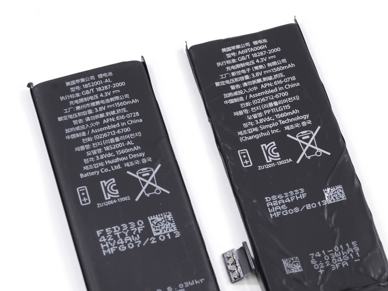
- as already confirmed, the battery of the iPhone 5S terminal has 1560 mAh, operating at 3.8V and offering 5.92 Whr;
- each of the 3 models of the iPhone 5S has batteries produced by different manufacturers, so there is the possibility of having differences in terms of autonomy;
- The Retina Display is identical to that of the iPhone 5;
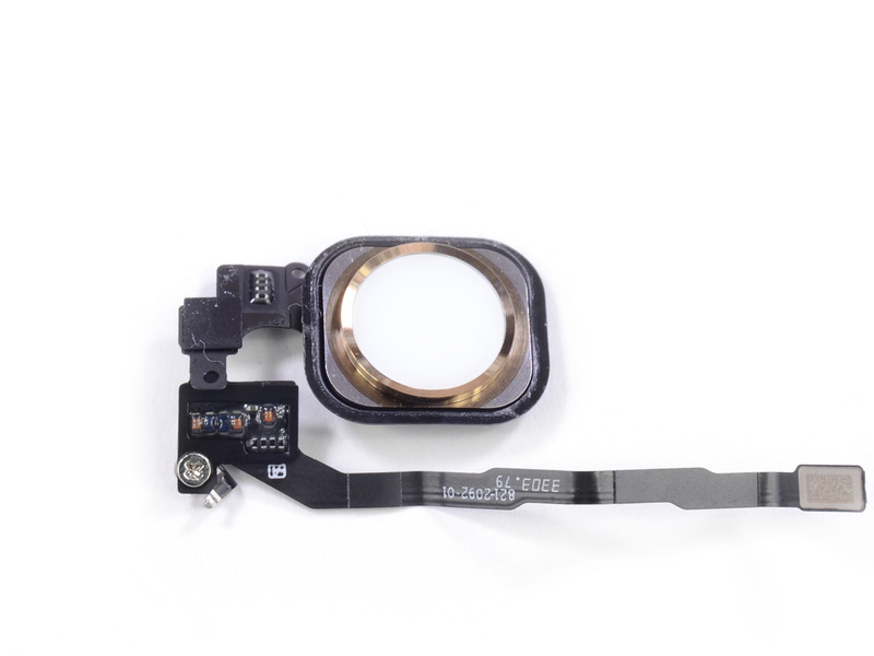
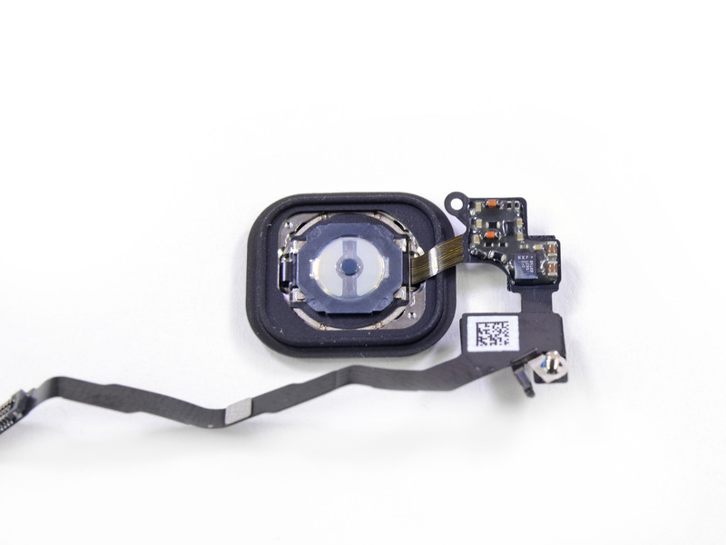
- the fingerprint reader has implemented a CMOS chip that registers the fingerprint;
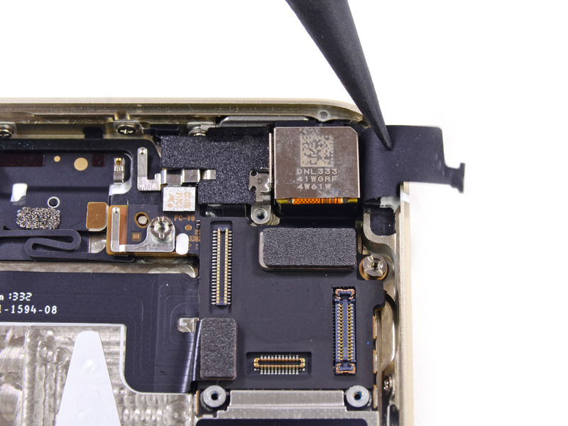
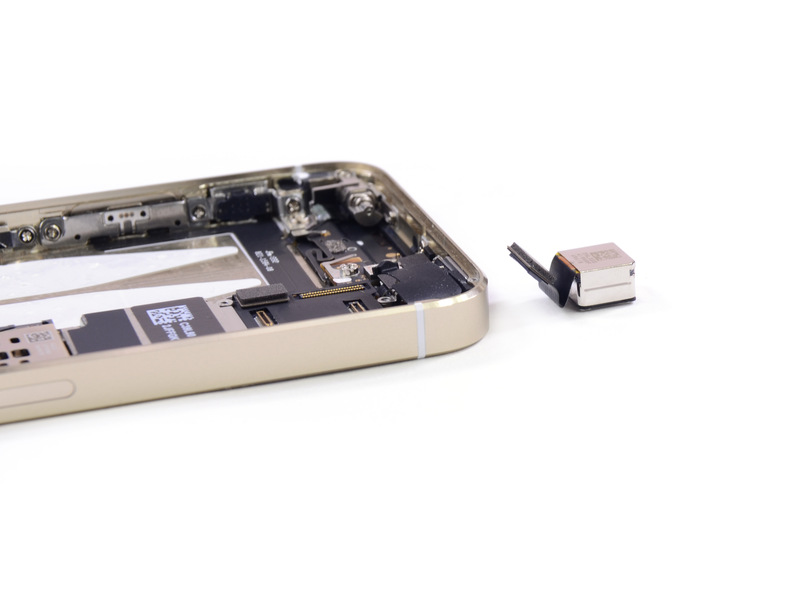
- the new iSight camera has the code DNL333 41WGRF 4W61W, apparently produced by Sony;
- the WiFi chip is Murata 339S0205, based on a Broadcom BCM4334 chip;
- the flash storage space in the iPhone 5S is produced by Hynix and has the code name SK Hynix H2JTDG8UD3MBR;
- The iPhone 5S is based on the A7 chip with the code name APL0698, a Qualcomm MDM9615M and a Qualcomm WTR1605L modem chip, and the interesting part is that that M7 chip cannot be seen inside the logic board;
That's about all I know about the iPhone 5S, so I'll leave you with the pictures.


